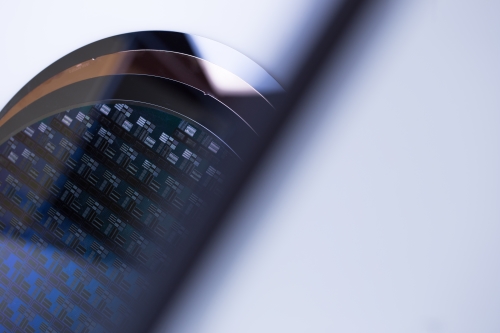
Silicon Wafers
The Active Business Company GmbH provides standardized and individual silicon wafers from well-known international Top Tier wafer manufacturers. We provide high-quality premium silicon products with numerous specifications. Almost everything can be done.

WAfer Specifications
• Silicon Wafer
• CZ and FZ
• 50 mm up to 450 mm
• different particle specifications
• Crystal orientation <100>, <110> and <111> and more on request
• different resistivities
• different thicknesses starting at 50 µm
• Surfaces: SSP, DSP, BSD, etched, coated
CZ-Wafer
CZ-Wafers (Silicon Wafer processed according to the Czochralski Method) are the mostly sold Silicon Wafers.
The tip of a rotating seed crystal is dipped in the doped silicon melt in a crucible. The seed crystal provides the desired crystal orientation. The result is a homogeneous boundary layer between the melt and the solid part of the seed crystal. The seed crystal is pulled up slowly as the melt solidifies at the forming interface. By varying pull rate and temperature, the growing crystal reaches the desired diameter. The arised crystal pillar is called an ingot.
FZ-Wafer
FZ-Wafers (Float Zone Silicon Wafer) are a high purity alternative to CZ-Wafers.
These wafers have a low concentration of impurities and high temperature capabilities. The FZ growth process begins with a multicrystalline silicon ingot that slowly rotates and passes through a heating element. A portion of the ingot is partially melted as the heating element moves along the ingot. As the silicon re-solidifies, the imperfections remain in the melted portion since these have a lower chemical potential. The heating element continues to rotate and move along the ingot. After the entire ingot passes through the heating element and dopants are added, it is cooled and sliced.
FZ-Wafers are commonly used in the manufacturing of discrete power devices, MEMS, diodes, RF-Devices, Thyristors and high efficiency solar cells.
Prime Wafers
The Active Business Company GmbH provides Prime Grade Wafers according to the Semiconductor Equipment and Materials International Standards (SEMIStd.) in all diameters from 1” up to 450 mm. Prime grade wafers are the highest possible grade of silicon wafer and can be used for device manufacturing with properties usually including extremely smooth surface and low Total Thickness Variation (TTV).
Test Wafers
The Active Business Company GmbH provides Prime Grade Wafers according to the Semiconductor Equipment and Materials International Standards (SEMIStd.) in all diameters from 1” up to 450 mm. Test grade wafers have a high quality but less stringent properties than prime grade wafers and are mostly used for equipment and fabrication testing.
Reclaimed Grade Wafers, Dummy Wafers
Reclaimed or Dummy Wafers are Prime or Test Wafers which have been processed already. Existing structures and coatings are removed chemically, the surface are polished again. The result is the same as Test Wafers and could be used in many applications, but with lower costs.
Our Advantages:
• long lasting, international network of leading silicon material manufacturers (Top Tier Manufacturer)
• large stock, small lot sizes, many specifications
• located in the European Union
• reduction of administrative expenses for the customer due to already declared commodity
• delivery free of charge
• delivery of small quantities possible
• high flexibility
• full service provider (one-stop shop for silicon material, coatings, applications and more)
Major Markets:
• Equipment manufacturers
• Chip manufacturers
• Opto-electronic industry
• MEMS
• R&D centers
• Universities
• Chemical industry
• Coating service provider

